Part Number : HY57V561620C
Function : 4 Banks x 4M x 16Bit Synchronous DRAM
Package : 54pin TSOP II Type
Maker : Hynix Semiconductor
Pinouts : 
Description :
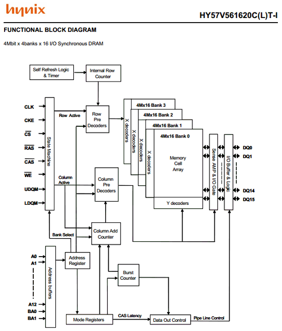
The HY57V561620C is a 268,435,456bit CMOS Synchronous DRAM, ideally suited for the main memory applications which require large memory density and high bandwidth. HY57V561620C is organized as 4banks of 4,194,304x16.
HY57V561620C is offering fully synchronous operation referenced to a positive edge of the clock. All inputs and outputs are synchronized with the rising edge of the clock input. The data paths are internally pipelined to achieve very high bandwidth. All input and output voltage levels are compatible with LVTTL.
Features
• Single 3.3±0.3V power supply
• All device pins are compatible with LVTTL interface
• JEDEC standard 400mil 54pin TSOP-II with 0.8mm of pin pitch (Leaded Package or Lead Free Package)
• All inputs and outputs referenced to positive edge of system clock
• Data mask function by UDQM, LDQM
• Internal four banks operation
Datasheet PDF Download : 
Others datasheet of same file :
HY57V561620, HY57V561620CLT-6I, HY57V561620CLT-8I,
HY57V561620CLT-HI, HY57V561620CLT-KI
